If you’ve ever held a sleek smartphone that folds neatly in half, a medical device that navigates tight, complex spaces in the human body, or an aerospace sensor that withstands intense vibration and temperature shifts, you’ve almost certainly interacted with a rigid-flexible PCB. As a supplier that’s spent the last 12 years working directly with engineers, designers, and product teams to build these boards, I’ve seen firsthand how much misunderstanding surrounds their manufacturing process. A lot of folks assume they’re just two separate PCBs glued together—nothing could be further from the truth. Rigid-flex PCBs are a hybrid technology that marries the durability of rigid FR-4 boards with the flexibility of polyimide (PI) or liquid crystal polymer (LCP) films, and their manufacturing is a precise, multi-step dance that requires equal parts precision engineering and specialized craftsmanship. Today, I’m pulling back the curtain on that process, walking you through what actually happens in our facility, where every single detail matters to the final product. Rigid-Flexible PCB
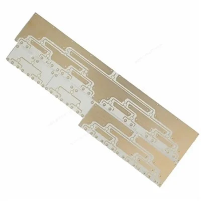
Before we even touch a piece of base material, the first step of manufacturing is critical: design and engineering validation. Too many teams jump straight to prototyping, only to hit costly roadblocks later, and that’s a mistake I see all the time. At our company, we work closely with our customers before any materials are cut or any machines are calibrated, because rigid-flex boards have unique design constraints that regular rigid PCBs don’t. For example, the flex zones—the areas that will bend during assembly, use, or installation—can’t have any vias, soldermask, or thick solder joints that would crack when flexed. We also have to account for the number of flex cycles a customer needs; a medical device that opens and closes 100,000 times in its lifetime needs a completely different flex zone design than an aerospace component that might only flex a handful of times in its 20-year lifespan. We use specialized EDA (electronic design automation) software that’s tailored for rigid-flex, like Allegro PCB Designer from Cadence and OrCAD, to map out layer stacks, flex boundaries, and connection points. We also run finite element analysis (FEA) simulations to test how the board will perform under real-world stress—bending, torsion, temperature fluctuations, vibration—before we ever cut a single material. This step often takes 10 to 15 business days for custom orders, but it saves our customers thousands in rework and replacement costs later.
Next comes the material preparation phase, which is where the core of the board’s structure is built. Rigid-flex PCBs have two types of base materials: rigid cores (almost always FR-4, a glass-reinforced epoxy laminate) and flexible dielectric films (usually polyimide, or PI, because it has excellent thermal stability, chemical resistance, and flexibility, though LCP is becoming more common for high-frequency applications like 5G). First, we cut these materials to size, using a high-precision laser cutter with a tolerance of ±0.05mm—any variation here throws off the entire layer stack. For the rigid sections, we sometimes add stiffeners (made of FR-4, aluminum, or steel) later to add rigidity where needed, but for now, we focus on the base materials. The flexible films are often supplied as rolls, since they’re thin and flexible, so we unroll them and cut them to match the rigid core dimensions for specific layer stacks. A key part here is aligning the material edges perfectly—we use precision edge guides and digital measurement tools to make sure every piece is straight, because even a 0.1mm misalignment will cause layers to shift during lamination, ruining the board.
Once the materials are cut and aligned, we move on to circuit patterning, which is where the conductive copper traces that carry electrical signals are formed. This step is split into two main processes for rigid-flex boards: subtractive and additive, though subtractive is far more common for high-volume, high-reliability orders. Let’s start with the rigid sections first, since they’re patterned the same way as standard rigid PCBs. We apply a layer of photoresist to the copper-clad rigid core, then expose it to UV light through a photomask that has the exact circuit pattern we designed earlier. The unexposed photoresist is then washed away, leaving a protective layer over the copper traces we want to keep. Next, we etch away the unwanted copper using a mild acid solution—this happens in a controlled environment where temperature and concentration are tightly regulated, because over-etching or under-etching can ruin the trace width and spacing, which is critical for signal integrity (especially for high-frequency boards). For the flexible sections, the process is slightly different. Flexible PI films are much thinner than rigid FR-4, so we use a more gentle etching process, often with a rotary etching machine, to avoid damaging the film. We also have to make sure the traces in the flex zones are slightly thicker than rigid traces? Wait no, actually—thinner traces in flex zones are better for flexibility, but they need to be durable enough to not break. So we calibrate the etching depth specifically for flex sections, usually around 1oz copper for rigid areas and 0.5oz or 1oz for flex, depending on the application. For very high-flex applications, we even use rolled copper instead of electrodeposited copper, because it’s more ductile and resists cracking better.
After patterning comes drilling, which is where holes are created for vias, component leads, and interconnections between layers. This is one of the most delicate steps in rigid-flex manufacturing, because we have to drill through both rigid and flexible materials, often alternating between them in the same stack. First, we use CNC drilling machines with ultra-small drill bits—some as small as 0.1mm—because rigid-flex boards have high layer counts, and we can’t have misaligned holes. For the flexible sections, drilling is even trickier: the thin PI film can tear if the drill bit applies too much pressure, so we use a vacuum hold-down system that applies just enough pressure to keep the material flat without stretching it. For small vias (less than 0.3mm), we also use laser drilling instead of mechanical drilling, because it’s more precise and causes less damage to the flexible dielectric. Once the holes are drilled, we de-burr them to remove any sharp edges from the drilling process—burrs can cause short circuits or damage to the flexible layers during later processing. We do a visual inspection of every drilled panel at this stage, using automated optical inspection (AOI) cameras that check for broken bits, misaligned holes, and burrs. Any panels that fail inspection are set aside for rework, and we’ve developed a special process for reworking small drill errors in flex zones, which is something many suppliers struggle with.
Next, we do plating, where we add a conductive layer to the holes so signals can pass between layers. For rigid-flex boards, we use a combination of electroless plating and electrolytic plating, same as rigid PCBs, but again, with adjustments for flexible materials. First, we treat the drilled panels with a palladium-based catalyst to make the hole walls conductive—this is called electroless plating, and it deposits a thin layer of copper that adheres to the hole walls. Then we do electrolytic plating, where we immerse the panel in a copper solution and apply an electric current, building up a thicker copper layer in the holes to ensure good conductivity and reliability. For flexible layers, we have to control the plating thickness very carefully; too much copper makes the flex zone stiff and prone to cracking, while too little causes high resistance in vias. We test the plating thickness of every panel using X-ray fluorescence (XRF) meters, which give us an accurate reading of copper thickness on hole walls and surfaces. After plating, we do another de-burring step and inspect the holes for voids or incomplete plating, which are common defects that cause board failure.
Now we get to one of the most defining steps of rigid-flex manufacturing: lamination. This is where all the rigid and flexible layers are bonded together into a single, solid board. Lamination is done in a high-temperature, high-pressure hydraulic press, and the process is extremely precise because we have to align each layer perfectly and avoid trapping air between layers, which causes voids or delamination. The materials used for lamination are either prepreg (a resin-impregnated fiberglass) for the rigid sections or acrylic adhesive for the flexible sections. For rigid layers, the prepreg melts under heat and pressure, bonding the FR-4 cores together. For flexible layers, the acrylic adhesive bonds the PI films to each other or to rigid sections. The lamination cycle is customized for each order: temperature is usually between 150°C and 180°C, pressure is between 200 and 500 psi, and the cycle time varies from 30 minutes to 2 hours, depending on the layer count. The flex zones are the biggest challenge here: if the pressure is too high, it can compress the flexible PI film, making it thick and inflexible; if it’s too low, the layers won’t bond properly. At our facility, we use custom-built lamination jigs that hold the flex zones flat while pressing the rigid sections, so the flexible areas maintain their thin profile and flexibility. We also use vacuum lamination for high-complexity boards, which removes air between layers before pressing, virtually eliminating voids. After lamination, we cool the boards slowly to avoid thermal stress, which can cause warping. Warping is a major issue with rigid-flex boards, especially for high layer counts, so we have a special cooling rack system that keeps the boards flat as they cool, preventing distortion.
Once the layers are laminated together, we move on to surface finishing, which protects the copper traces from oxidation and prepares the board for component assembly. Rigid-flex boards use the same surface finishes as standard PCBs, but with specific considerations for flex zones. The most common finishes are ENIG (Electroless Nickel Immersion Gold) and ENEPIG (Electroless Nickel Electroless Palladium Immersion Gold), which provide good solderability and wear resistance. For flex zones, we avoid finishes that are too thick or rigid, like immersion tin, because it cracks when bent. We also sometimes use organic solderability preservative (OSP) for low-reliability applications, but it’s not ideal for boards that will flex repeatedly, as it wears off over time. We apply the surface finish in a continuous line, because rigid-flex panels are often cut from rolls for flexible sections, so our line is designed to handle both rigid and flexible substrates without damaging the layers. After surface finishing, we apply solder mask to the rigid sections and any non-flex areas. Solder mask is a protective layer that covers unwanted copper, prevents short circuits, and gives the board its green (or other custom color) finish. For flex zones, we do not apply solder mask, or we apply a thin, flexible solder mask that won’t crack when bent. This is another critical step—too thick a solder mask in a flex zone will cause the board to fail in as few as 100 flex cycles, so we use a specialized flexible solder mask material and a spray-on application process that only deposits a thin, even layer on rigid sections.
Next comes silkscreen printing, where we add component designators, part numbers, and other markings to the board. This is pretty similar to standard PCBs, but again, we avoid printing in flex zones, since the ink can crack and flake off during bending. We use UV-cured inks that are flexible enough for non-flex areas, and we do a rubbing test after printing to make sure the ink adheres properly. After silkscreen, we do another round of testing: AOI, which checks for defects in the solder mask, silkscreen, and surface finish, and X-ray inspection, which looks for hidden defects like voids in plated vias or misaligned internal layers. For high-reliability orders, like medical or aerospace, we also do a flying probe test, which sends small probes into contact with every test point on the board to check for continuity, short circuits, and open traces. We run this test at multiple points in the process, too—not just at the end—so we can catch defects early and avoid wasting time on assembly of a faulty board.
Finally, after all testing passes, we do the final cut and forming of the board. Most rigid-flex boards are routed from a larger panel, using a CNC router with bits that are sized to avoid damaging the flex zones. For very small or intricate boards, we use laser cutting, which is more precise and creates a clean edge without burrs. We also do any forming here, like bending the flex zones to a specific angle, though most forming is done after component assembly by our customers. Wait, actually—some customers ask us to do partial forming for high-volume orders, so we have custom bending jigs that hold the board at a specific angle without putting too much stress on the flex zone. After cutting and forming, we do a final visual inspection and a flex test, where we bend a sample of each board’s flex zone 100 times (or the number of cycles the customer specified) to make sure no traces crack or vias fail. We also test for continuity before packaging, so we’re confident the board works before it leaves our facility.
At the end of the day, manufacturing rigid-flex PCBs is about balancing precision with flexibility—literally. Every step requires adjustments that don’t matter for standard rigid PCBs, and even the smallest mistake can cause a board to fail when it’s put to use. Over the years, we’ve refined our process by working directly with customers across industries—medical, aerospace, automotive, consumer electronics—to solve their unique challenges, and that’s what sets our boards apart from the competition. Rigid-flex technology is only going to get more important as products get smaller, lighter, and more durable, and as we move toward more flexible smartphones, wearable medical devices, and autonomous vehicles that rely on compact, high-performance electronics.

If you’re designing a new product that could benefit from a rigid-flex PCB—whether you’re a startup working on a wearable, an aerospace engineer building a satellite sensor, or a medical device designer creating a next-gen surgical tool—I’d love to help. Our team has 12 years of specialized experience in rigid-flex design, prototyping, and manufacturing, and we work with you every step of the way to make sure your board is reliable, meets your specifications, and fits within your budget. Don’t hesitate to reach out to start the conversation about your project.
FR4 PCB References
- Johnson, H., & Graham, M. (2011). High-Speed Signal Integrity. Prentice Hall.
- Electronic Industries Alliance (EIA). (2019). Standard for Rigid-Flex and Flex Printed Wiring Boards (EIA-416-A).
- Liu, Y., et al. (2020). Mechanical reliability of flexible printed circuit boards under cyclic bending. IEEE Transactions on Components, Packaging and Manufacturing Technology.
- Cadence Design Systems. (2022). Allegro Rigid-Flex PCB Design User Guide.
Fastline Circuits Co., Limited
Fastline Circuits Co., Limited is one of the most professional rigid-flexible PCB manufacturers and suppliers in China. With abundant experience, we warmly welcome you to wholesale durable rigid-flexible PCB made in China here and get quotation from our factory. All customized products are with high quality and competitive price.
Address: Room 301, Building B3, Fuqiao 4th District, Qiaotou Community, Fuhai Subdistrict, Bao’an District, Shenzhen, Guangdong Province, China
E-mail: sales@fastlinepcb.com
WebSite: https://www.fastlinepcb.net/
